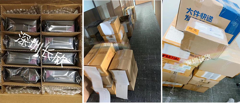
WhatsApp:+86 18150087953 WeChat: +86 18150087953
  Email:
Description
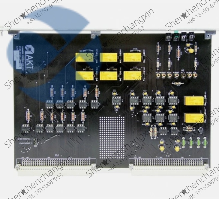
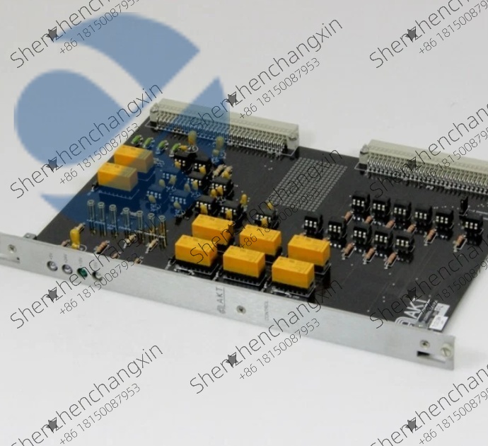
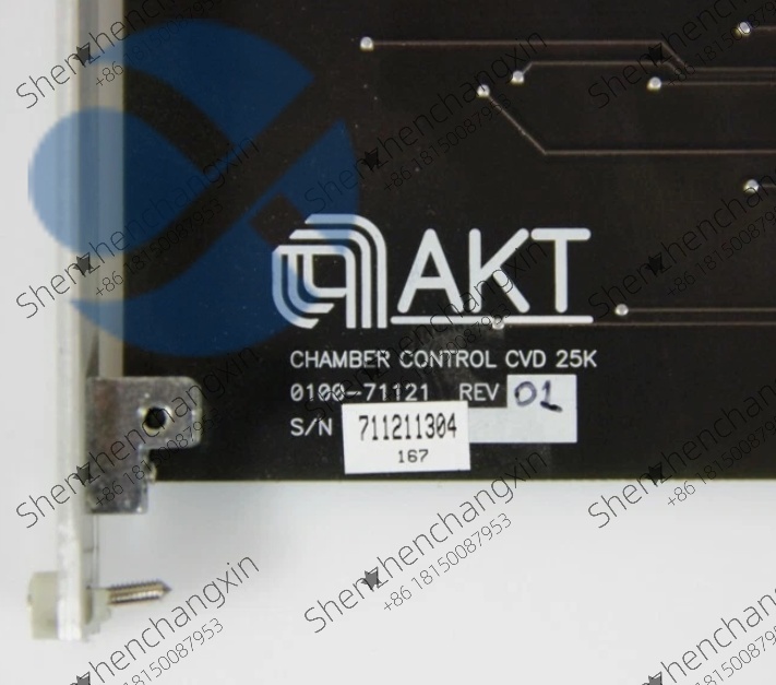
AMAT Applied Materials AKT Chamber Control CVD 25K Board(0100-71121 Rev.02):The Chamber Control Core of Semiconductor CVD Equipment
In the chemical vapor deposition(CVD)process of semiconductor manufacturing,the chamber control circuit board is the”nerve center”that ensures thin film deposition accuracy,process stability,and safe equipment operation.AMAT Applied Materials,a semiconductor equipment giant,offers the Chamber Control CVD 25K Board(Model 0100-71121 Rev.02)specifically for its AKT series CVD equipment.With its nanometer-level process parameter control capabilities,high anti-interference performance,and deep compatibility with AKT CVD equipment,it has become a core control component for high-end manufacturing applications such as 12-inch wafers and flexible display panels.Whether depositing oxide layers on silicon wafers or preparing encapsulation layers for flexible OLEDs,this circuit board ensures a stable process environment within the CVD chamber through precise coordinated control of temperature,pressure,and gas flow,providing critical hardware support for the performance and yield of semiconductor devices.
1.Hardware Design and Core Parameters:A Structural Foundation of Semiconductor-Grade Precision
1.1 Semiconductor-Grade Hardened Hardware Architecture
The AMAT AKT Chamber Control CVD 25K Board(0100-71121 Rev.02)utilizes a high-cleanliness hardware design specifically designed for semiconductor equipment.Measuring approximately 220mm×160mm×25mm,it fits into the dedicated control card slot of the AKT series CVD equipment.Gold-plated pins provide a low-impedance connection to the equipment’s main controller(contact resistance≤30mΩ),ensuring attenuation-free transmission of high-frequency process signals.The board’s surface is lead-free gold-plated,meeting the electromagnetic compatibility requirements of the SEMI F47 standard.It also offers chemical resistance,withstanding long-term corrosion from trace corrosive gases(such as ammonia and silane)around the CVD chamber,preventing contact failures caused by oxidation of the metal pins.
The board integrates multiple high-precision functional modules:the core control unit utilizes a TI TMS320C6000 series high-speed DSP chip(operating frequency≥1GHz),supporting multi-channel parallel processing of process parameters;the analog signal conditioning circuit utilizes the ADI AD8628 ultra-low offset voltage operational amplifier(offset voltage≤1μV)to ensure nanometer-level signal acquisition;the digital signal interface is equipped with a TI SN75176 differential transceiver,supporting interference-resistant transmission over the RS485 industrial bus;and a built-in ADI AD7799 24-bit high-precision ADC(analog-to-digital converter)enables high-resolution acquisition of process parameters.The board edges are equipped with anti-fouling positioning pins and electrostatic discharge(ESD)protection components(protection level±15kV contact discharge)to prevent installation errors and damage to chips caused by static electricity.This is particularly critical in the dry environment of semiconductor cleanrooms(where the risk of static electricity is high).1.2 Key Electrical and Process Control Parameters
Parameter Category
Specifications
Product Model
AMAT Applied Materials AKT Chamber Control CVD 25K Board(0100-71121 Rev.02)
Manufacturer
Applied Materials
Product Type
Specialized circuit board for chamber control of semiconductor CVD equipment(process parameter acquisition and control execution)
Compatible Equipment
AMAT AKT series CVD equipment(such as the AKT 25K and AKT 30K,used for 12-inch wafer/flexible display panel manufacturing)
Core Processor
TI TMS320C6000 series DSP(operating frequency≥1 GHz)
Process Parameter Control Channels
8 analog inputs(temperature/pressure/gas flow),6 analog outputs(actuator control),12 digital inputs/outputs(equipment status monitoring/safety interlock)
Analog Input Accuracy
24-bit ADC,measurement accuracy±0.001%Full-scale range(temperature:±0.1°C,pressure:±0.01 Torr,gas flow:±0.1 sccm)
Analog output accuracy:16-bit DAC,output accuracy:±0.005%full-scale(control signal:4-20mA/0-5V DC)
Digital signal standard:24V DC PNP(compatible with semiconductor device safety standards)
Communication interface:RS485(process data transmission),SPI(intra-board module communication),EtherCAT(high-speed synchronization with the device main controller)
Supply voltage:±15V DC(analog circuit),+5V DC(digital circuit),ripple factor≤0.1%
Operating environment requirements:Temperature:20°C to+25°C(cleanroom constant temperature requirement),Humidity:30%to 50%RH(non-condensing),Cleanliness level:Class 10(compliant with SEM IS2 standards)
Immune to interference:Common-mode rejection ratio(CMRR)≥130dB,electromagnetic emission(EMI)complies with EN 61614-1:2008 61326-1(Electromagnetic Compatibility Standard for Semiconductor Equipment)
Safety Certifications
SEMI S2/S8(Safety Standard for Semiconductor Equipment),CE,UL
Firmware Version
Compatible with AMAT AKT CVD equipment firmware V5.0 and above
2.Core Function:Driving Precision Process Control of the CVD Chamber
2.1 Coordinated Control of Multiple Process Parameters
The core advantages of the AMAT AKT Chamber Control CVD 25K Board(0100-71121 Rev.02)lie in”nanoscale process parameter acquisition”and”dynamic coordinated control of multiple parameters.”Eight analog input channels,through dedicated signal conditioning circuitry,can simultaneously acquire key process parameters within the CVD chamber.For example,during the silicon wafer oxide(SiO₂)deposition process,the board collects chamber heater temperature(via an RTD sensor,ranging from 25°C to 800°C),chamber pressure(via a capacitive pressure sensor,ranging from 0.1 to 10 Torr),and reactant gas(such as O₂and SiH₄)flow rates(via a mass flow controller(MFC),ranging from 0 to 500 sccm).The high resolution of the 24-bit ADC ensures that temperature fluctuations as small as 0.1°C,pressure changes as small as 0.01 Torr,and flow rate deviations as small as 0.1 sccm can be captured,providing precise raw data for the DSP chip’s process algorithms.Six analog output channels directly drive chamber actuators:Based on DSP calculations,they output 4-20mA signals to control the heating stage power regulator(maintaining temperature stability),the pressure control valve(adjusting chamber pressure),and the MFC valve(precisely controlling gas flow ratio).For example,during the deposition process of the flexible OLED encapsulation layer(SiNx),if the chamber pressure drops by 0.05 Torr due to gas leakage,the board can adjust the pressure control valve output signal within 10ms to correct the pressure deviation to within±0.01 Torr,preventing pinhole defects in the encapsulation layer.Furthermore,12 digital channels enable equipment status monitoring and safety interlocking:digital inputs capture chamber door status and vacuum pump operation signals.If a”chamber door is not securely closed,”a digital output triggers an emergency shutdown,cutting off the reactant gas supply and preventing hazardous gas leaks—fully complying with the safety requirements of the SEMI S8 standard.2.2 Deep Collaboration with AKT CVD Equipment
As the native control card for the AMAT AKT series CVD equipment,the 0100-71121 Rev.02 achieves hardware-level synchronization with the equipment’s main controller without the need for third-party drivers.The card connects to the main controller via EtherCAT,with a data update cycle of≤1ms,ensuring real-time synchronization of process parameters and control commands.This is particularly critical in wafer batch production.For example,during the deposition process of a batch of 25 12-inch wafers,the main controller uses the card to adjust the chamber temperature compensation value for each wafer in real time(due to temperature variations caused by wafer position differences).The card responds and executes temperature adjustment commands within 0.8ms,ensuring film thickness deviation of≤5nm across the batch(the industry standard is≤10nm).The board supports”process recipe storage and recall”functionality:connecting to the onboard Flash memory(capacity≥128MB)via the SPI interface,it can store over 100 different process recipes(such as SiO₂,SiNx,and Poly-Si deposition parameters).Once a technician selects a recipe through the device’s user interface,the board loads all parameters(temperature setpoints,pressure thresholds,and gas flow ratios)within 50ms,eliminating the need for recalibration and significantly reducing process changeover time.For example,in a semiconductor foundry,switching from wafer oxide deposition to metal passivation deposition can be reduced from 30 minutes to 5 minutes,increasing equipment utilization by 15%.In addition,the board features an online firmware upgrade function:it receives firmware update packages from the master controller(obtained from the official AMAT server)via the EtherCAT bus.This allows upgrades without disassembling the hardware,ensuring the board’s functionality is synchronized with the device firmware version.For example,the newly added”process parameter trend prediction”function analyzes historical data to provide early warning of temperature drift risks(such as temperature deviations caused by heating stage aging),preventing batches of wafers from being scrapped.2.3 Fault Self-Diagnosis and Semiconductor-Grade Reliability
To meet the stringent”zero downtime”requirements of semiconductor manufacturing,the board incorporates a multi-level fault diagnosis and protection mechanism.The board monitors its hardware status(DSP operating status,ADC/DAC accuracy,and power supply voltage)in real time.If it detects that the accuracy of an analog input channel exceeds±0.001%of full scale(for example,a temperature acquisition deviation of 0.5°C),it immediately sends a fault code(such as”0x08-ADC Channel 3 Accuracy Exceeded”)to the main controller via RS485.This triggers a red fault indicator on the board and automatically switches to a backup control channel(for example,switching temperature acquisition to a backup RTD sensor),ensuring uninterrupted processing.For example,in a wafer fab’s SiO₂deposition process,the board detects an abnormal signal from the primary pressure sensor and switches to the backup sensor within 0.5ms,preventing wafer scrapping due to chamber pressure loss and reducing losses by approximately 50,000 yuan per batch.For reliable power supply,the board utilizes dual isolated±15V/5V power inputs.If a single power supply fails,the backup power supply seamlessly takes over within 2ms.The power module also features overvoltage and overcurrent protection(overvoltage thresholds:±18V/6V,overcurrent thresholds:2A/5A),preventing voltage fluctuations from damaging precision chips.Furthermore,the board has passed SEMIS2 lifespan testing:at a constant temperature of 20°C to 25°C,the mean time between failures(MTBF)is≥50,000 hours,far exceeding the 30,000-hour standard for industrial-grade equipment.This ensures that the board can operate continuously for three years(with annual maintenance)for semiconductor equipment.
3.Typical Application Scenarios:Covering High-End Semiconductor Manufacturing
3.1 12-inch Wafer Oxide(SiO₂)Deposition
In the gate oxide process of semiconductor logic chip manufacturing,the AMAT AKT 25K CVD equipment deposits 5-10nm thick SiO₂films on 12-inch silicon wafers.The 0100-71121 Rev.02 board performs core control tasks:it uses analog inputs to acquire heating stage temperature(target 700°C±0.1°C),chamber pressure(target 2 Torr±0.01 Torr),O₂flow rate(target 200 sccm±0.1 sccm),and SiH₄flow rate(target 50 sccm±0.1 sccm).It uses analog outputs to control heating stage power(maintaining temperature stability),the pressure control valve(correcting pressure deviations),and the MFC valve(adjusting gas ratios).Digital channels monitor chamber door status and vacuum pump operation signals.After implementing this board,oxide layer thickness uniformity improved from±3%to±1.5%,meeting the gate insulation requirements of 7nm process chips.The thickness variation within a wafer batch decreased from 8nm to 4nm,and the yield increased from 92%to 97%,reducing annual wafer scrap losses by approximately 2 million yuan.A semiconductor foundry reported that the board’s failure rate was only 0.2 failures per year,significantly lower than the 1.5 failures per year for comparable third-party boards,and increased equipment utilization by 3%.
3.2 Deposition of the Flexible OLED Encapsulation Layer(SiNx)
In the manufacture of flexible OLED display panels,a SiNx encapsulation layer(500-1000nm thick)is deposited using a CVD process to prevent moisture and oxygen from corroding the panel’s pixel structure.The AMAT AKT 30K CVD system,equipped with the 0100-71121 Rev.02 board,enables low-temperature deposition control on flexible substrates(such as PI films).Analog inputs capture chamber temperature(target 150°C±0.5°C;flexible substrates are not resistant to high temperatures),pressure(target 5 Torr±0.05 Torr),NH₃flow rate(target 300 sccm),and SiH₄flow rate(target 100 sccm).Analog outputs control the power of the infrared heating tubes(to prevent local overheating and substrate deformation),the pressure regulating valve,and the MFC valve.Digital channels trigger the start and stop signals of the substrate transport mechanism.The board’s low-temperature temperature control accuracy(±0.5°C)ensures no cracking risk in the SiNx encapsulation layer.Water vapor permeability is reduced from 1×10⁻⁴g/(m²・day)to 5×10⁻⁵g/(m²・day),extending the lifespan of OLED panels from 30,000 hours to 50,000 hours.After implementation at a display panel manufacturer,the defect rate in the encapsulation process dropped from 4.5%to 1.2%,reducing panel scrap by approximately 5,000 units per month.3.3 Power Semiconductor Epitaxial Layer(SiC)Deposition